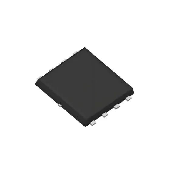
90mΩ, 650V GaN HEMT With Integrated Driver and Protection
1. FEATURES
- 650V enhancement mode HEMT with integrated driver
- 90mΩ RDSON
- 5V PWM input
- UVLO protection
- Zero reverse recovery
- Low quiescent current driver
- Adjustable turn-on slew rate
- Dv/Dt immunity both with/without driver-supply
- Low propagation delay for up to 2MHz operation
2.APPLICATIONS and TECHNOLOGIES
- As switching FETs in singles, or in pairs as half-bridges
- AC-DC, DC-DC, DC-AC converters
- PFC applications (totem pole and standard)
- High frequency LLC converters
- Mobile chargers and laptop adapters
- LED and motor drives
- Server power supplies
3.Description
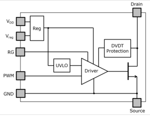
The DTQ13N65GN is a 90mΩ, 650V GaN HEMT device with integrated driver circuit. The monolithic integration of driver minimizes inductance in the gate loop enabling safe
and clean switching even at high-voltage high-frequency operations.
This device makes the applications more efficient/reliable, and also reduces the size of the magnetic components dramatically. UVLO function of the device turns-off the HEMT in case VDD voltage droops below its threshold voltage. A proprietary dv/dt protection circuit protects the HEMT from drain-dvdt induced false turn-on even in the absence of VDD supply. An external resistance between Vreg and RG allows control of drain voltage slew rate for best EMI performance.
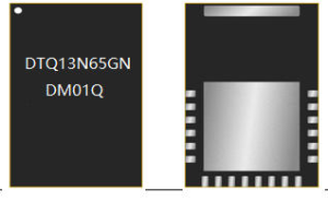
4.Pin Definition
| Pin Number | Pin Name | Pin Type | Description |
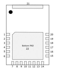
| 1, 7-20 | NC | No connect. Pins 8-20 can be connected to GND for better PCB layout. Pin 1 and Pin 7 should be left open. | |
| 2 | VDD | LV-PWR | VDD supply for driver. Connect 7.5V with a bypass capacitor of 220nF. |
| 3 | Vreg | AO | Internally generated supply. Connect a bypass capacitor of 22nF. |
| 4 | RG | AI | Connect a suitable resistor between RG and Vreg for controlling the drain voltage slew rate during the turn on. |
| 5 | PWM | DI | PWM input |
| 6 | GND | GND | Ground pin of the driver (internally Kelvin connected to the source of the 650V GaN HEMT) |
| 21 | Drain | HV-PWR | Drain of 650V GaN HEMT |
| 22 (Back Pad) | Source | Source of 650V GaN HEMT |

