To understand a MOSFET’s “capabilities,” its performance parameters are critical. These specs dictate circuit efficiency, speed, and reliability—from smartwatches to EV charging stations, every parameter impacts design success. Below are six key metrics that define MOSFET performance:
1. Threshold Voltage (V<sub>GS(th)</sub>)
Definition: The minimum gate-to-source voltage required to turn the MOSFET “on” (create a conductive channel).
Significance: Lower V<sub>GS(th)</sub> reduces driver power consumption but compromises noise immunity. IoT devices often use low thresholds (1-2V), while industrial systems favor higher thresholds (3-4V) to withstand voltage noise.
2. On-Resistance (R<sub>DS(on)</sub>)
Definition: Resistance between the drain and source when the MOSFET is fully ON.
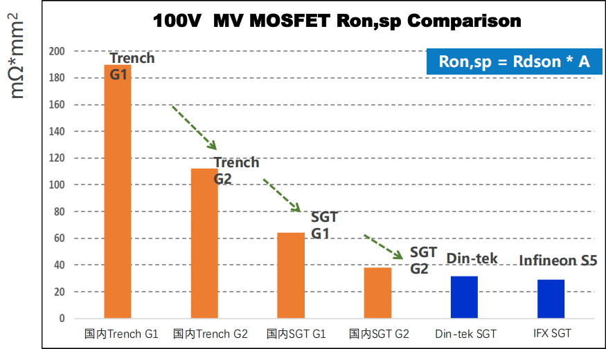
Critical Impact: R<sub>DS(on)</sub> determines conduction losses (I²R), especially in high-current applications. Din-Tek’s advanced MOSFETs employ trench-gate technology, reducing R<sub>DS(on)</sub> to milliohm levels—minimizing heat and extending battery life.
Din-Tek’s cutting-edge packaging and ultra-thin wafer processing technologies minimize Rds(on), unlocking unprecedented efficiency in power management.

3. Switching Speed (t<sub>r</sub>/t<sub>f</sub>)
Definition: Rise time (t<sub>r</sub>) and fall time (t<sub>f</sub>) measure how quickly the MOSFET transitions between ON/OFF states.
Core Value: Faster switching boosts efficiency in high-frequency applications (e.g., DC-DC converters), but excessive speed can trigger voltage spikes. Din-Tek devices balance speed and EMI performance through optimized packaging and driver design.
4. Maximum Drain-Source Voltage (V<sub>DSS</sub>) and Current (I<sub>D</sub>)
Safety Limits: V<sub>DSS</sub> is the maximum voltage the drain-source can withstand, while I<sub>D</sub> is the continuous current rating. Exceeding these causes permanent damage. Designers should select MOSFETs with a 20% margin (e.g., 15V+ for a 12V system). Din-Tek offers silicon carbide (SiC) MOSFETs rated up to 1500V for high-voltage renewable energy systems.
5. Gate Charge (Q<sub>g</sub>)
Hidden Cost: Total charge required to charge/discharge the gate capacitance during switching. Higher Q<sub>g</sub> increases driver power loss, crippling efficiency at high frequencies. Din-Tek’s gallium nitride (GaN) MOSFETs reduce gate charge by 80% versus silicon, ideal for 5G base stations and fast-charging solutions.
6. Thermal Resistance (R<sub>θJA</sub>)
Thermal Management: Measures how efficiently heat flows from the chip to the environment. Lower R<sub>θJA</sub> means better heat dissipation. For example, TO-220 packages have R<sub>θJA</sub> ~62°C/W, while Din-Tek’s copper-clip packaging slashes this to 15°C/W—tripling power density.
Why Do These Parameters Matter?
In motor control, low R<sub>DS(on)</sub> reduces heat; in server PSUs, low Q<sub>g</sub> and high switching speed break efficiency barriers. Selecting a MOSFET is an art of balancing trade-offs—and Din-Tek’s experts tailor solutions to your needs.
From Parameters to Performance: Din-Tek Delivers Zero Compromise
Whether you need ultra-low-loss Si MOSFETs or high-frequency SiC/GaN solutions, Din-Tek Semiconductor combines cutting-edge technology and real-world data to empower your designs.
Drop us an email, sarah@dintek-semi.com, for free samples and a comprehensive selection guide—Find Your Ultimate MOSFET Today! ⚡


