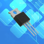
From the beginning to the completion of manufacturing of semiconductor products, there are two main processing processes, which are called front-end production and back-end production. Although MOSFET is a semiconductor device with a relatively simple structure, it also needs to go through these two production processes.
Front-end production mainly refers to wafer manufacturing, including complex processing steps such as photolithography, plasma etching, ion implantation, ion diffusion, oxidation, evaporation, vapor phase epitaxial growth, sputtering and chemical vapor deposition. The purpose of these processing steps It mainly creates crystal grains with complete functions on silicon wafers. The electrical properties of each grain
Yes, it can be verified by the wafer test platform built by the probe station and automatic test equipment. It cannot pass the test.
The grains will be marked with ink dots as unqualified marks. These marks will be identified in subsequent production.
The inked die will not be processed. Since the wafer is called a wafer or die, the test on the die is also called
Wafer Sorting or Die Sorting.
Back-end production mainly refers to packaging testing, that is, through the processing process shown in Figure 1-1, the die is manufactured into the style we usually see. When the product is packaged, it needs to be tested again to verify the electrical performance of the product. Ensure that the finished product meets product specifications. Since this test is the last process of post-production,
It is also the last step of the entire production process, so it is called the final test, that is, Final Test.
A brief introduction to the packaging and testing preparation process is as follows:
1) Wafer Sawing.
Use a high-speed rotating cutting knife to cut and separate the grains on the wafer.
2) Die Attach.
Silver glue sticks the die to the predetermined position of the lead frame.
3) Wire Bond.
Between the solder joints of the die and the pins of the lead frame, thin metal wires are welded to establish the connection between the die circuit and the outside.
4) Molding.
Place the pin pivot with the die attached and the melted wires into the die-casting mold, then press the molten resin plastic into the mold, and wrap the entire die according to the packaging requirements.
5) Cutting and forming, Trim and Form.
Cut off excess connecting material from the lead frame, and shape the leads into the required shape according to the product’s packaging form.
6) Final Test.
Test whether the performance of the product meets the requirements. Products that pass the test are considered qualified products
Although there are certain process control methods and quality monitoring methods in each packaging process, there are still some defects that are difficult to control and are introduced into the product. Therefore, after the product is packaged, it needs to be tested to identify the quality of the product. In terms of test items and test methods, the difference between Wafer Sorting and Final Test is not big, but the final test is at the last step of the entire production and processing process. The role of product quality control is even more important.
Din-Tek Semiconductor is professional MOSFET designer and manufacturer. All parts will be tested strictly by QA process. Welcome you to come us for checking. Any questions, please kindly drop us an email, sarah@dintek-semi.com.


